It is clear that the polarization fields play a critical role in AlGaN/GaN HEMTs and are the primary source of the sheet charge density in the devices. Therefore, to obtain a precise estimation for the sheet charge density in the heterojunction, we calculate the sheet charge density based on a model that accounts for the nonlinearity of the spontaneous and piezoelectric polarization as functions of the Al composition. In order to model the sheet charge density correctly in the heterostructure under an applied gate voltage, we solve the Poisson and Schroedinger equations self-consistently at the heterojunction. The 3D free carriers and the partial neutralization of donors are directly taken into account in place of the usual assumption of fully ionized donors in the doped layer. The details of the formula are described in [17-19]. The electron density distribution n(z) in the Poisson equation includes distribution of the 2D (n2D) and 3D (n3D) electron densities.
(1)
Only the 3D free carrier concentration in the barrier layer is taken into account. Nc is the effective density of 3D states in the conduction band. F1/2 is the Fermi-Dirac integral of order 1/2, and vc(z) is the electron potential in the conduction band. The ionized donor concentration (z) in the device is given by
(2)
where ED is the donor level measured from the conduction band edge.
The polarization effects can be incorporated into the model by the boundary condition at the hetero-interface. The boundary condition is specified as follows. The electric displacement must be continuous at the hetero-interface yielding
(3)
where Pis the sum of spontaneous and piezoelectric polarization, e and V are the dielectric constant and potential, respectively. At the metal-semiconductor interface the potential energy above the Fermi level is the Schottky barrier height. At the substrate the Fermi energy is assumed to lie at midgap in the undoped GaN.
The calculation procedure as shown in Fig.1 will be briefly described as follows. For an initial guess potential, we solve the Schroedinger equation to obtain the subband energy levels and wave functions in the quantum well. Then the sheet charge density can be calculated from the 2D electron density function. It is noted that the Fermi energy Ef is set to a reference level and set equal to zero [17]. Therefore, the conduction band profile which satisfies the boundary condition can be obtained from solving the Poisson equation. For the next iteration, the effective potential energy function is calculated from a linear combination of new and old potential energy by a factor a. The factor a is a relaxation constant and is generally adjusted to obtain a smooth convergence. Also the 3D free electrons and ionized donor concentration are updated by equations (1)-(2). Then the effective potential energy function is used to calculate new wave functions. The procedure is repeated until the effective and old potential energy within the same iteration differ by less than a specified error.


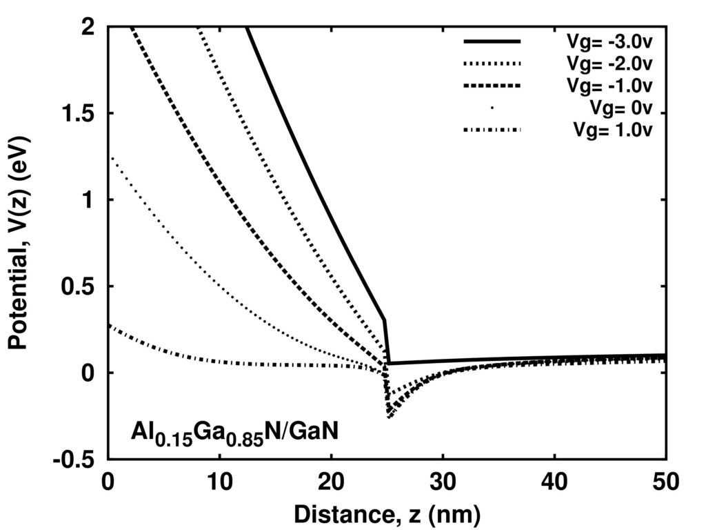
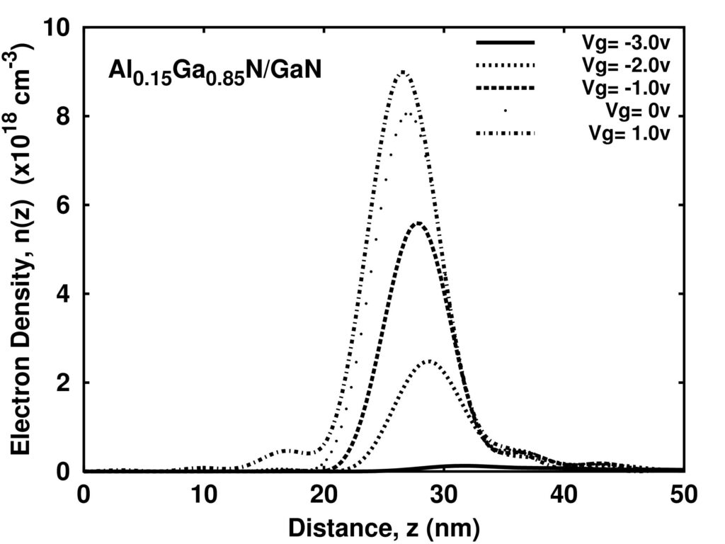
Figures 2 and 3 show self-consistent results for the AlGaN/GaN HEMT at room temperature for the conduction band profile and confined carrier concentration in the channel, respectively. The structure and doping concentrations of the AlGaN/GaN HEMT device considered in these plots are described in Table I. The Fermi level is set to zero in Figure 2. At the gate voltage of –3V, the device is actually depleted near the Al0.15Ga0.85N/GaN interface. Therefore, there is no charge density confined in the 2D channel. As the gate voltage increases, the band bending becomes sharper and thus the carrier concentration in the channel increases. A further increase of the gate voltage mainly increases the number of electrons in the Al0.15Ga0.85N layer, either as bound electrons or as 3D free electrons.
The ionized donor concentration as a function of gate bias at the Al0.15Ga0.85N/GaN hetero-interface is shown in Figure 4. At a gate bias of –3V, the donors are fully ionized in the AlGaN layer while as the gate voltage switches to positive the donor ionization becomes incomplete. On the other hand, once the gate voltage switches to positive biases, the 2D channel is formed quickly. A significant increase of the electrons in the 2D channel corresponds to a drop in the ionized donor concentration near the hetero-interface.
As the channel voltage increases from the source to the drain in HEMT devices, the channel gradually becomes a bulk-like structure. Therefore, the velocity-field characteristics of bulk material are used in our simulation. The bulk GaN velocity-field characteristics based on a previous Monte Carlo simulation are used in our calculation. To express the strong field-dependent mobility, we use an analytical formula determined by least-square curve fitting as
(4)
where e is the applied electric field and v1, e1, a, b, and z are curve fitting parameters extracted from our Monte Carlo simulation [16] and m0 is the zero-field mobility. The expression given in eq. 4 has the same functional form that we used to model a GaN/AlGaN heterostructure [16]. Owing to the fact that the bulk GaN velocity field curve and that for a GaN/AlGaN heterostructure are relatively close, it is reasonable to use the same functional form for the velocity field relationship but with different parameters. The quantity εc is the critical field whose value is also chosen in order to obtain the best fit to experiment. If the electric field is less than the critical electric field, the velocity follows the analytical formula. Once the channel electric field exceeds the critical field, the velocity is assumed to saturate at a value equal to that of the peak velocity. The equation, however, can not lead to an analytical form for the I-V characteristics while it can be numerically solved in the quasi-2D model.
For example, the velocity-field characteristics in our GaN HEMT simulation are shown in Fig.5. The parameters v1, e1, a, b, x, and m0 are 2.35×107 cm/s, 161 kV/cm, 17.98, 0.917, 1.88, and 500 cm2/V-s and Vsat and ec are 2.69×107 cm/s and 150 kV/cm, respectively in equation (4). Notice the good agreement between the Monte Carlo calculated drift velocity and that obtained by use of Eq.(4) as shown in Figure 5.
For the AlGaAs/GaAs HEMT, the velocity-field is obtained from the well-known formula [20],
(5)
In this case the parameters used are selected to give the best agreement between the calculated results for the current-voltage characteristic and the experimental data. The values used are discussed in Section III.
The current-voltage calculation in HEMT devices is based on a quasi-2D model [9,21-26], which is a good trade-off between the complexity of the full 2D models and the simplicity of analytical models. Based on the self-consistent charge control model and velocity-field characteristics, the drain current can be obtained from the current continuity equation. To simplify the calculation we neglect the diffusion term in the drain current calculation. Basically, the channel region under the gate can be divided into uniform sections and the source and drain contact resistances are connected to the source and drain end regions. For a given drain current, the channel voltage, channel carrier concentration, carrier velocity, and the channel electric field in each section can be calculated from the source terminal to the drain end. Therefore for a given drain current, we can obtain its corresponding drain voltage. Once the channel electric field exceeds the critical field, the drain current is assumed to saturate. The detailed calculation formulas are shown in Ref.15.
In addition, the transconductance and current-gain cutoff frequency also are included in our simulation. Three kinds of carrier concentration contribute to the gate to source capacitance. These are the carrier concentration for the 2DEG, free carriers and neutralized donors in the barrier layer [27].