In this article, we have presented calculations of the DC and RF characteristics in comparable AlGaN/GaN and AlGaAs/GaAs HEMTs. The sheet charge density calculations for different gate biases are made using a self-consistent solution of the Schroedinger and Poisson equations. The carrier mobility in the GaN HEMT is extracted from previous Monte Carlo simulations. A quasi-2D model is then used to calculate the drain-current voltage characteristics. The effects of the spontaneous and piezoelectrically induced polarization fields in the AlGaN/GaN HEMT are incorporated into the model by the boundary condition at the hetero-interface. That is the electric displacement must be continuous at the hetero-interface. The model used to characterize the AlGaN/GaN HEMT device is based on a nonlinear polarization model since the macroscopic polarization of nitride alloys is indeed nonlinear as a function of composition. Since a fair comparison of the GaAs and GaN HEMTs requires comparable device structures, we have chosen a device structure for which experimental data are available for GaAs. Unfortunately, no experimental data for this particular structure in GaN exists. Therefore, the model is calibrated for the GaAs calculation to experimental data. Previous calculations were made comparing the GaN calculations to experiment but for different structures. Nevertheless, excellent agreement was obtained between the model and experiment for GaN HEMTs indicating that the model can be successfully employed to the study of GaN HEMTs. Using this model, we have examined six different performance measures for GaN and GaAs HEMTs. The six performance measures are the sheet carrier concentration, capacitance-voltage characteristics, maximum drain current at similar gate and drain bias, pinch-off voltage, transconductance and cutoff frequency. It is found that the maximum drain current and the magnitude of the pinch-off voltage in the GaN device are larger than those in the GaAs device due to a significantly larger sheet charge induced by the polarization field at the hetero-interface. On the other hand, the maximum transconductance in the GaAs device is higher than that in the GaN device. This is because the low-field mobility in the GaAs HEMT is significantly larger than that in the GaN HEMT. Also increments of the sheet charge in the 2D channel with respect to a variation of the gate voltage (DQ2DEG/DVg) in the GaAs device are higher than that in the GaN device. Both of these two factors cause a higher peak transconductance in the GaAs device. The maximum cutoff frequency is very close in these two devices since the GaAs device has a larger Cgs corresponding to its peak gm. However, the transconductance in the GaN device decreases slowly as the gate voltage switches to a forward bias. This indicates that the GaN device can be employed in a larger voltage swing. Consequently, the GaN HEMT exhibits the potential for high power and high frequency applications.
Category: Carrier transport
Comparison between AlGaN/GaN and AlGaAs/GaAs HEMTs
To make a comparison between AlGaN/GaN and AlGaAs/GaAs HEMTs, we consider a representative AlGaAs/GaAs HEMT structure that consists of a 3nm undoped Al0.27Ga0.73As spacer and a 27nm thick Al0.27Ga0.73As doped layer with a doping level of 2×1018 cm-3 [28]. The same geometry structure and doping level in the doped layer are used in the Al0.15Ga0.85N/GaN HEMT. The material compositions are chosen so as to yield a structure with similar conduction band edge discontinuities and comparable well depths. The conduction band discontinuities are 0.286V and 0.25V are for the Al0.27Ga0.73As/GaAs and Al0.15Ga0.85N/GaN HEMT, respectively. The material parameters used in the calculation are compiled in Ref. 15 Table I.
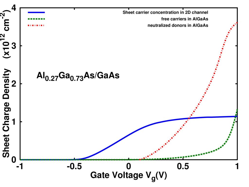
Figures 6 and 7 show the calculated sheet carrier concentration as a function of gate voltage in the Al0.27Ga0.73As/GaAs and Al0.15Ga0.85N/GaN heterostructures, respectively. The free electrons and neutralized donors in the doped layer are calculated by integrating n3D(z) and in equations (1)-(2) over the barrier thickness. As the gate voltage increases, the free electrons in the 2D channel tend to go into the doped layer as 3D free electrons or to neutralize the donors. Therefore, the sheet carrier concentration in the 2D channel saturates, which limits the maximum voltage swing in the HEMTs. The maximum sheet charge density of 5.12×1012 cm-2 in the Al0.15Ga0.85N/GaN heterostructure is significantly larger than that of 1.14×1012 cm-2 in the Al0.27Ga0.73As/GaAs heterostructure due to a larger polarization field induced at the AlGaN/GaN hetero-interface. Also, to deplete this larger sheet charge at the hetero-interface, the threshold voltage in the GaN device becomes more negative, corresponding to a larger voltage swing.
The gate capacitance is calculated by differentiating the sheet charge density under the gate with respect to the applied gate voltage. The calculated capacitance per unit area is shown in Figures 8 and 9 as a function of gate bias for the Al0.27Ga0.73As/GaAs and Al0.15Ga0.85N/GaN heterostructures respectively. The curve denoted by C2DEG is the capacitance due to electrons in the 2D channel, C3D is due to electrons in the AlGaAs or AlGaN layer, and CNeu is due to neutralized donors in the barrier. As can be seen from Figures 8-9, near the threshold voltage, donors throughout the doped layer are fully ionized with no free electrons in the barrier, and 2D electrons are distributed deep into the GaAs or GaN channel, resulting in a small capacitance. As the gate voltage increases, the capacitance increases quickly because of the band bending and an increase in the confined electrons induced by the gate voltage. Once the 2DEG is formed, the effective position of the 2DEG from the hetero-interface is no longer noticeably influenced. Hence, the capacitance remains almost constant in a small voltage range around the maximum capacitance. When the gate voltage is further forward biased, donor neutralization and parallel conduction become significant. As a consequence, the capacitance due to the 2DEG in the channel decreases while the total capacitance increases. It is noted that the peak capacitance of 0.276 mF/cm2 due to 2DEG in the GaAs device is larger than that of 0.247 mF/cm-2 in the GaN device. The peak capacitance in the GaAs device is higher than that in the GaN device since in the GaAs device the gate voltage alone mainly controls the sheet charge. In contrast within the GaN device it is the combined effect of the polarization field and the gate voltage that controls the sheet charge. In addition, as the gate voltage is further forward biased, the total gate capacitance in the GaAs device increases rapidly. Thus the cutoff frequency drops quickly as the gate voltage increases.
A comparison of the I-V characteristics for the Al0.27Ga0.73As/GaAs and Al0.15Ga0.85N/GaN HEMTs is shown by Figures 10-11. As can be seen from Figure 10, the calculated I-V characteristic of the Al0.27Ga0.73As/GaAs HEMT is plotted along with experimental measurements [28]. Relatively good agreement between the experimental data and simulation results is obtained. To obtain the best agreement with the experimental data, the critical field ec, saturation velocity vsat, and the low-field mobility m0 in Eq.(5) used in the model are 3.5×10⁵ V/m, 1.6×107 cm/s, and 9,143 cm2/V-s, respectively. The maximum sheet carrier concentration has been set to1.08×1012 cm-2 for gate voltages greater than 0.5V. To consider a finite output conductance, the drain current is multiplied by (1+lVDS) in the saturated current regime [29]. Here l is the fitting parameter and is 0.07 in this calculation. Furthermore, the source and drain resistances are also taken into account and have been adjusted to 6W.
The maximum drain current of 66.3 mA at a gate bias of 0.9V and a drain bias of 5V in the Al0.15Ga0.85N/GaN HEMT is larger than that of 36.3 mA for the Al0.27Ga0.73As/GaAs HEMT with the same biases. The conducting channel within the Al0.15Ga0.85N/GaN device closes-off completely at Vgs = -3.98V with a drain current as low as 1.0 mA/mm at Vds=5V. The corresponding voltage in the Al0.27Ga0.73As/GaAs device is Vgs = -0.44V. Moreover, in the Al0.15Ga0.85N/GaN HEMT, the on-off state current ratio of 663 is larger than that of 363 in the Al0.27Ga0.73As/GaAs HEMT.
The transconductance and cutoff frequency for both devices are shown in Figure 12 at a drain bias of 5V. The maximum transconductance of 292 mS/mm in the Al0.27Ga0.73As/GaAs device with a Vgs= 0.175V and Ids=124 mA/mm is larger than that of 187 mS/mm in the Al0.15Ga0.85N/GaN HEMT with a Vgs= -1V and Ids=347 mA/mm. The maximum gm is influenced by two factors: capacitance due to 2DEG and low-field mobility. The 2DEG capacitance indicates how much charge can be supplied to the 2D channel with respect to a variation of the gate voltage. The excess supply charge directly contributes to an increase of the drain current. Therefore, the maximum gm strongly depends on the peak of the 2DEG capacitance. The maximum 2DEG capacitance of the Al0.27Ga0.73As/GaAs device is larger than that of Al0.15Ga0.85N/GaN structure as shown in Figures 8-9. In addition to the modulation of charge in the 2D channel, the electrons in the channel are not all traveling at the saturated or peak electron velocity except those at the drain edges. Hence, gm is also proportional to the low-field mobility. The low-field mobility of 9143 cm2/V-s in the Al0.27Ga0.73As/GaAs device is significantly larger than that of 500 cm2/V-s in the Al0.15Ga0.85N/GaN device in this plot. Therefore, both these two factors cause a higher peak transconductance in the Al0.27Ga0.73As/GaAs device. However, the Al0.15Ga0.85N/GaN device still exhibits a transconductance of 146 mS/mm at a drain current of 663 mA/mm and a gate bias of 0.9 V. For the GaAs device, the transconductance drops more precipitously at 0.9 V gate bias to a value of 66.3 mS/mm.
Consequently, the GaN HEMT has a larger useful voltage swing implying better high power performance.
Figure 12 also shows the calculated cutoff frequency as a function of gate voltage for the GaAs and GaN HEMT structures. When the gate is forward biased, the parallel conduction and donor neutralization cause a decrease of gm and also lead to an increase of Cgs. Therefore, the cutoff frequency falls off at forward biases. As can be seen from Figure 12, the maximum cutoff frequency (fT)max of 13.8 GHz in the GaN device is very closed to that of 13.6 GHz in the GaAs device. This difference is attributable to the fact that the value of Cgs corresponding to (fT)max in the GaN device is less than that in the GaAs device.
Model Description
It is clear that the polarization fields play a critical role in AlGaN/GaN HEMTs and are the primary source of the sheet charge density in the devices. Therefore, to obtain a precise estimation for the sheet charge density in the heterojunction, we calculate the sheet charge density based on a model that accounts for the nonlinearity of the spontaneous and piezoelectric polarization as functions of the Al composition. In order to model the sheet charge density correctly in the heterostructure under an applied gate voltage, we solve the Poisson and Schroedinger equations self-consistently at the heterojunction. The 3D free carriers and the partial neutralization of donors are directly taken into account in place of the usual assumption of fully ionized donors in the doped layer. The details of the formula are described in [17-19]. The electron density distribution n(z) in the Poisson equation includes distribution of the 2D (n2D) and 3D (n3D) electron densities.
(1)
Only the 3D free carrier concentration in the barrier layer is taken into account. Nc is the effective density of 3D states in the conduction band. F1/2 is the Fermi-Dirac integral of order 1/2, and vc(z) is the electron potential in the conduction band. The ionized donor concentration (z) in the device is given by
(2)
where ED is the donor level measured from the conduction band edge.
The polarization effects can be incorporated into the model by the boundary condition at the hetero-interface. The boundary condition is specified as follows. The electric displacement must be continuous at the hetero-interface yielding
(3)
where Pis the sum of spontaneous and piezoelectric polarization, e and V are the dielectric constant and potential, respectively. At the metal-semiconductor interface the potential energy above the Fermi level is the Schottky barrier height. At the substrate the Fermi energy is assumed to lie at midgap in the undoped GaN.
The calculation procedure as shown in Fig.1 will be briefly described as follows. For an initial guess potential, we solve the Schroedinger equation to obtain the subband energy levels and wave functions in the quantum well. Then the sheet charge density can be calculated from the 2D electron density function. It is noted that the Fermi energy Ef is set to a reference level and set equal to zero [17]. Therefore, the conduction band profile which satisfies the boundary condition can be obtained from solving the Poisson equation. For the next iteration, the effective potential energy function is calculated from a linear combination of new and old potential energy by a factor a. The factor a is a relaxation constant and is generally adjusted to obtain a smooth convergence. Also the 3D free electrons and ionized donor concentration are updated by equations (1)-(2). Then the effective potential energy function is used to calculate new wave functions. The procedure is repeated until the effective and old potential energy within the same iteration differ by less than a specified error.
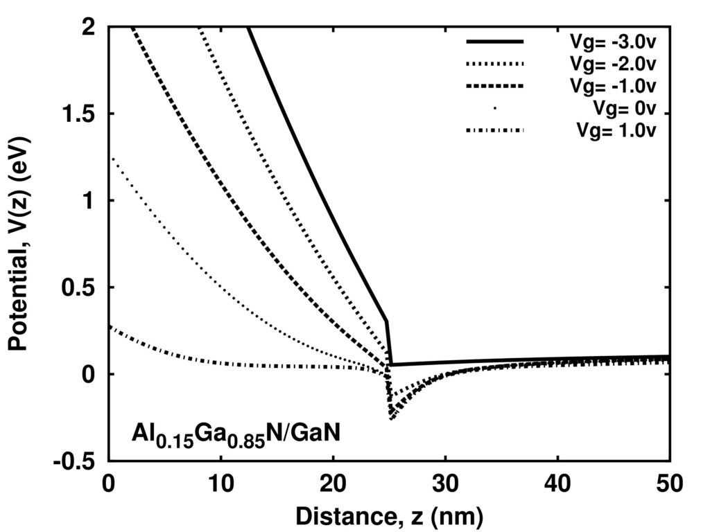
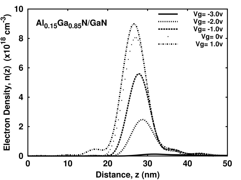
Figures 2 and 3 show self-consistent results for the AlGaN/GaN HEMT at room temperature for the conduction band profile and confined carrier concentration in the channel, respectively. The structure and doping concentrations of the AlGaN/GaN HEMT device considered in these plots are described in Table I. The Fermi level is set to zero in Figure 2. At the gate voltage of –3V, the device is actually depleted near the Al0.15Ga0.85N/GaN interface. Therefore, there is no charge density confined in the 2D channel. As the gate voltage increases, the band bending becomes sharper and thus the carrier concentration in the channel increases. A further increase of the gate voltage mainly increases the number of electrons in the Al0.15Ga0.85N layer, either as bound electrons or as 3D free electrons.
The ionized donor concentration as a function of gate bias at the Al0.15Ga0.85N/GaN hetero-interface is shown in Figure 4. At a gate bias of –3V, the donors are fully ionized in the AlGaN layer while as the gate voltage switches to positive the donor ionization becomes incomplete. On the other hand, once the gate voltage switches to positive biases, the 2D channel is formed quickly. A significant increase of the electrons in the 2D channel corresponds to a drop in the ionized donor concentration near the hetero-interface.
As the channel voltage increases from the source to the drain in HEMT devices, the channel gradually becomes a bulk-like structure. Therefore, the velocity-field characteristics of bulk material are used in our simulation. The bulk GaN velocity-field characteristics based on a previous Monte Carlo simulation are used in our calculation. To express the strong field-dependent mobility, we use an analytical formula determined by least-square curve fitting as
(4)
where e is the applied electric field and v1, e1, a, b, and z are curve fitting parameters extracted from our Monte Carlo simulation [16] and m0 is the zero-field mobility. The expression given in eq. 4 has the same functional form that we used to model a GaN/AlGaN heterostructure [16]. Owing to the fact that the bulk GaN velocity field curve and that for a GaN/AlGaN heterostructure are relatively close, it is reasonable to use the same functional form for the velocity field relationship but with different parameters. The quantity εc is the critical field whose value is also chosen in order to obtain the best fit to experiment. If the electric field is less than the critical electric field, the velocity follows the analytical formula. Once the channel electric field exceeds the critical field, the velocity is assumed to saturate at a value equal to that of the peak velocity. The equation, however, can not lead to an analytical form for the I-V characteristics while it can be numerically solved in the quasi-2D model.
For example, the velocity-field characteristics in our GaN HEMT simulation are shown in Fig.5. The parameters v1, e1, a, b, x, and m0 are 2.35×107 cm/s, 161 kV/cm, 17.98, 0.917, 1.88, and 500 cm2/V-s and Vsat and ec are 2.69×107 cm/s and 150 kV/cm, respectively in equation (4). Notice the good agreement between the Monte Carlo calculated drift velocity and that obtained by use of Eq.(4) as shown in Figure 5.
For the AlGaAs/GaAs HEMT, the velocity-field is obtained from the well-known formula [20],
(5)
In this case the parameters used are selected to give the best agreement between the calculated results for the current-voltage characteristic and the experimental data. The values used are discussed in Section III.
The current-voltage calculation in HEMT devices is based on a quasi-2D model [9,21-26], which is a good trade-off between the complexity of the full 2D models and the simplicity of analytical models. Based on the self-consistent charge control model and velocity-field characteristics, the drain current can be obtained from the current continuity equation. To simplify the calculation we neglect the diffusion term in the drain current calculation. Basically, the channel region under the gate can be divided into uniform sections and the source and drain contact resistances are connected to the source and drain end regions. For a given drain current, the channel voltage, channel carrier concentration, carrier velocity, and the channel electric field in each section can be calculated from the source terminal to the drain end. Therefore for a given drain current, we can obtain its corresponding drain voltage. Once the channel electric field exceeds the critical field, the drain current is assumed to saturate. The detailed calculation formulas are shown in Ref.15.
In addition, the transconductance and current-gain cutoff frequency also are included in our simulation. Three kinds of carrier concentration contribute to the gate to source capacitance. These are the carrier concentration for the 2DEG, free carriers and neutralized donors in the barrier layer [27].
Introduction
Due to the superior material properties such as high breakdown voltage, high saturation velocity, and high thermal conductivity, III-nitride devices are expected to offer better high frequency, high power, and high temperature performance compared to conventional Si and GaAs devices. The AlGaN/GaN high electron mobility transistor (HEMT) is one of the most promising devices because of its modulation-doped structure and a significantly larger polarization field induced at the hetero-interface. Recent progress in growth and process technology has already led to very impressive results for AlGaN/GaN HEMTs. A transconductance as high as 270 mS/mm has been achieved in devices with 0.7 μm gate length [1]. AlGaN/GaN HEMTs grown on a SiC substrate with a power density as high as 9.8 W/mm at 8 GHz have also been demonstrated, which is about ten times higher than GaAs-based FETs [2], and current gain cutoff frequencies of 101 GHz have been reported [3]. Recent studies show that there is about a 20% deviation for the sheet charge density in the AlGaN system between theoretical predictions and experimental measurements [4]. Nitride device modeling [5-10] has assumed that the polarization in nitride alloys is linearly interpolated from the values of the parent binary compounds [11-12]. However, recent research indicates that the macroscopic polarization in III-nitride alloys is a nonlinear function of the material composition [4]. Moreover, recent experimental measurements in AlGaN/GaN heterostructures illustrate that reasonable agreement is obtained using the nonlinear polarization formulation [4,13-14]. Also our research has shown that excellent agreement between the simulation and experimental data is obtained when the nonlinear polarization formulation is employed in the AlGaN/GaN HEMT model [15].
Since both the spontaneous and piezoelectric polarization fields can induce a significantly larger sheet charge and alter the band bending at the AlGaN/GaN hetero-interface, the device performance in the AlGaN/GaN HEMT is quite different from that in the AlGaAs/GaAs HEMT. Therefore, it is important to make a comparison between AlGaN/GaN and AlGaAs/GaAs HEMTs to illustrate how this natural advantage translates into improved device performance.
Several theoretical AlGaN/GaN HEMT simulation models have been presented and reported in the literature [5-10]. Rashmi’s group presented analytical models including a one-dimensional (1D) and two-dimensional (2D) model to examine DC and RF characteristics of HEMTs [5-7]. A full band Monte Carlo simulation also was presented by Ando et al [8]. Sacconi et al. investigated DC performance by using a quasi-2D model [9]. Within the framework of the gradual channel approximation, Albrecht et al. included the thermal effects in the I-V calculation of a GaN/AlGaN HEMT [10]. Though much progress has been made by these researchers, to the author’s knowledge this is the first theoretical study of the comparison between AlGaN/GaN and AlGaAs/GaAs HEMTs with the same basic geometric structure. The AlGaN/GaN HEMT model includes a nonlinear formulation of the polarization effects [15].
In order to affect a reasonable comparison of the AlGaAs/GaAs and AlGaN/GaN HEMTs comparable device structures must be examined. Unfortunately, experimental data are only available for the specific structure examined for the AlGaAs/GaAs HEMT. Thus the AlGaAs/GaAs HEMT device calculation is calibrated by using measured data. In an earlier work, we have compared our calculations of AlGaN/GaN HEMTs to other structures for which experimental data were available [15]. Excellent agreement was obtained thus ensuring that the present calculations for the AlGaN/GaN device have also been calibrated albeit to different device structures.
The sheet charge density, a function of gate voltage, is calculated from the Schroedinger and Poisson equations self-consistently. The carrier mobility in the AlGaN/GaN HEMT is extracted from Monte Carlo simulation [16]. Based on the self-consistent charge control model and the field-dependent mobility, a quasi-2D model is used to calculate the drain-current characteristics in the HEMT devices. The most important characteristics including the sheet charge density vs. gate voltage, gate to source capacitance, drain current-voltage, transconductance, and cut-off frequency are used to examine the performance of GaN and GaAs HEMTs.
III-V UTB Performance
III-V UTB nMOSFET Performances
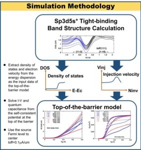
Top-of-the-barrier (TOB) simulation methodology
Ballistic performance

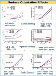
Surface orientation effects
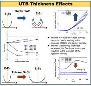
UTB thickness effects
Non-coherent
Non-coherent transport
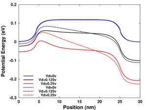
Potential energy
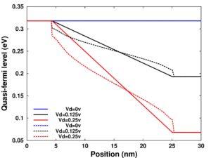
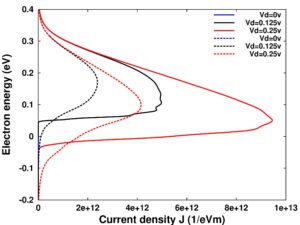
Solid and dashed lines represent ballistic and scattering transport, respectively.
Quasi-fermi level
Current density
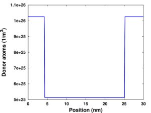
Donor atoms for n++-n+-n++ resistor
Charge density
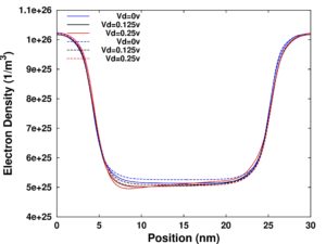
Ballistic
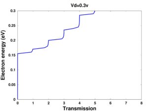
Use non-equilibrium Green’s function (NEGF) to simulate ballistic multi-subband transmission
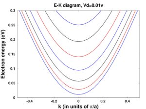
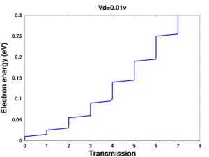
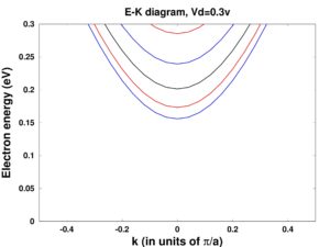
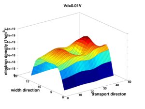
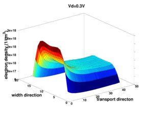
Drain voltage impact on channel electron density
